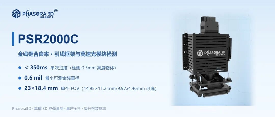
In Parts 1 and 2, we unpacked the production limits of DoF stacking and the underlying logic of Phasora3D’s patented multi-layer focus tracking (displacement imaging). This post goes to engineering: how the PSR2000 series turns that architecture into a real-line solution for gold-wire-bonding pain points at OSATs.
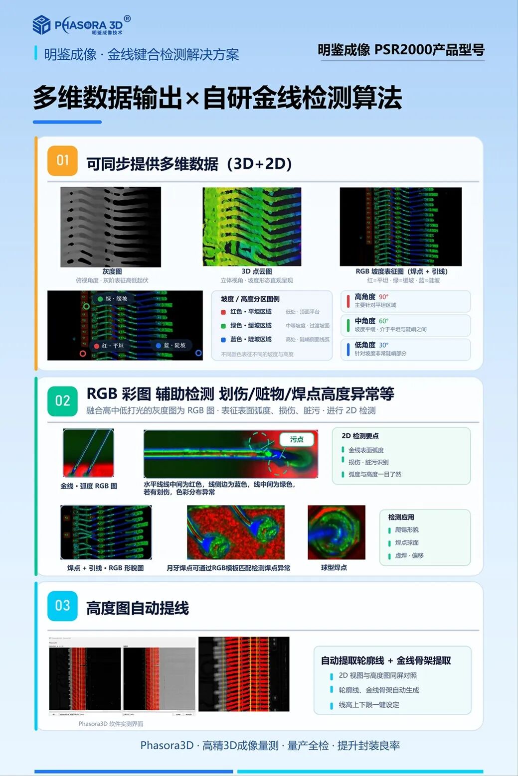
One scan, same-source 2D + 3D data
The PSR2000 series outputs multi-dimensional data from a single scan, closing the gaps of standalone 2D or standalone 3D:
- Same-source 2D + 3D output: grayscale image, 3D point cloud, and RGB slope map are captured from the same source — eliminating image-registration errors from multi-camera setups while delivering morphology, height, and slope features in one pass.
- RGB slope color map reveals invisible surface defects: catches wire scratches, contamination, crescent/ball-bond deformation, and bond-height anomalies that pure height measurement easily misses.
- Automatic wire-loop extraction from the height map: the algorithm traces the wire loop and loop skeleton, with configurable loop-height thresholds for instant detection of abnormal loop height, wire sag, and bond misalignment — eliminating human error and heavy manual tracing.
Key specs: minimum measurable gold wire 0.6 mil, repeatability up to 1 μm — covering memory-chip bonding, two-tier stacked chips, high-speed optical modules, and lead frames.
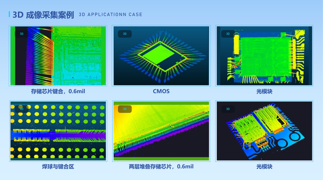
Proven on the production line
From Phasora3D’s published test cases:
- Memory-chip ultra-fine wire inspection: 3D morphology inspection + surface defect recognition on 0.6 mil gold wires in a single pass.
- Stacked-chip inspection: layered imaging — upper and lower wires do not interfere, and each bonding layer is evaluated independently.
- High-speed optical modules & lead frames: high-throughput inline inspection, combining 3D metrology with bond-surface defect recognition.
Many 3D systems on the market are fit only for lab sampling. The PSR2000 series was designed for mass-production inline 100% inspection from day one — helping OSATs cut material scrap from escaped defects and reduce the manual re-inspection cost of false calls.
Three questions to ask in vendor selection
As Chiplet and high-density bonding scale, choosing a 3D inspection system is no longer about picture clarity. Ask three core questions:
- Are micro-defects being smoothed away by the algorithm?
- Does processing speed meet inline 100%-inspection takt?
- Does it output same-source 2D + 3D data for comprehensive defect classification?
DoF stacking still has a place in lab sampling and analysis — but micro-defect loss from pixel fusion is a fundamental, inherent limitation. Built on patented multi-layer focus tracking, the Phasora3D PSR2000 series combines layered raw imaging, millisecond-level processing, and same-source multi-dimensional data to address real production pain points in ultra-fine wire, stacked packaging, and high-speed optical module inspection. It also signals that China’s 3D imaging industry is moving beyond parameter benchmarking toward original innovation at the imaging-principle level.
Learn more: www.phasora3d.com