


CORE PRODUCTS
核心产品
面向半导体先进封装与精密电子制造,提供高精度 3D 与 3D+2D 同步光学量测。


- 20+
- 自主知识产权/多项PCT国际专利
- 双中心
- 苏州·新加坡协同布局,覆盖海内外业务
- 源于工艺
- 从真实工艺痛点出发,定义行业标品
使命
致力于提升CoWoS工艺良率,为AI算力铸就基石。
价值观
坚守自主创新、客户为本的发展理念。
核心战略
围绕高端封装工艺需求,搭建全链条3D成像模组。
发展目标
主导半导体封装量产全检3D成像系统新标准。
APPLICATIONS
应用场景
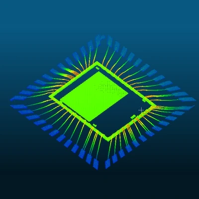
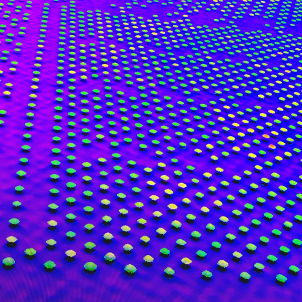
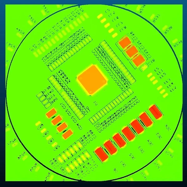
覆盖微组装、引线框架、微型锡膏及 PCBA/BGA 的四类真实检测应用。

OUR TEAM / 芯片协同
把复杂问题,拆成一张系统图
芯片、算法和软件在同一张图上对齐,让每一个判断都能被验证。


研发团队讨论芯片方案
NEWSROOM
新闻动态
PSR2000 Series Tech Brief #3 | Gold Wire Bonding Inspection: The PSR2000 Production Solution — and How to Choose
In Parts 1 and 2, we unpacked the production limits of DoF stacking and the underlying logic of Phasora3D's patented multi-layer focus tracking (displacement imaging). This post goes to engineering: how the PSR2000 series turns that architecture into a real-line solution for gold-wire-bonding pain points at OSATs.
阅读详情PSR2000 Series Tech Brief #2 | Multi-Layer Focus Tracking: Ditch the Synthetic "Perfect Picture" — Preserve Real Defect Data on the Line
In our last post, we explained why full depth-of-focus (DoF) stacking — built on pixel fusion plus global smoothing — traps gold-wire-bonding 100% inspection in a triple bind: escaped defects, false calls, and throughput shortfalls. Resolving this contradiction means rethinking the imaging foundation itself.
阅读详情