
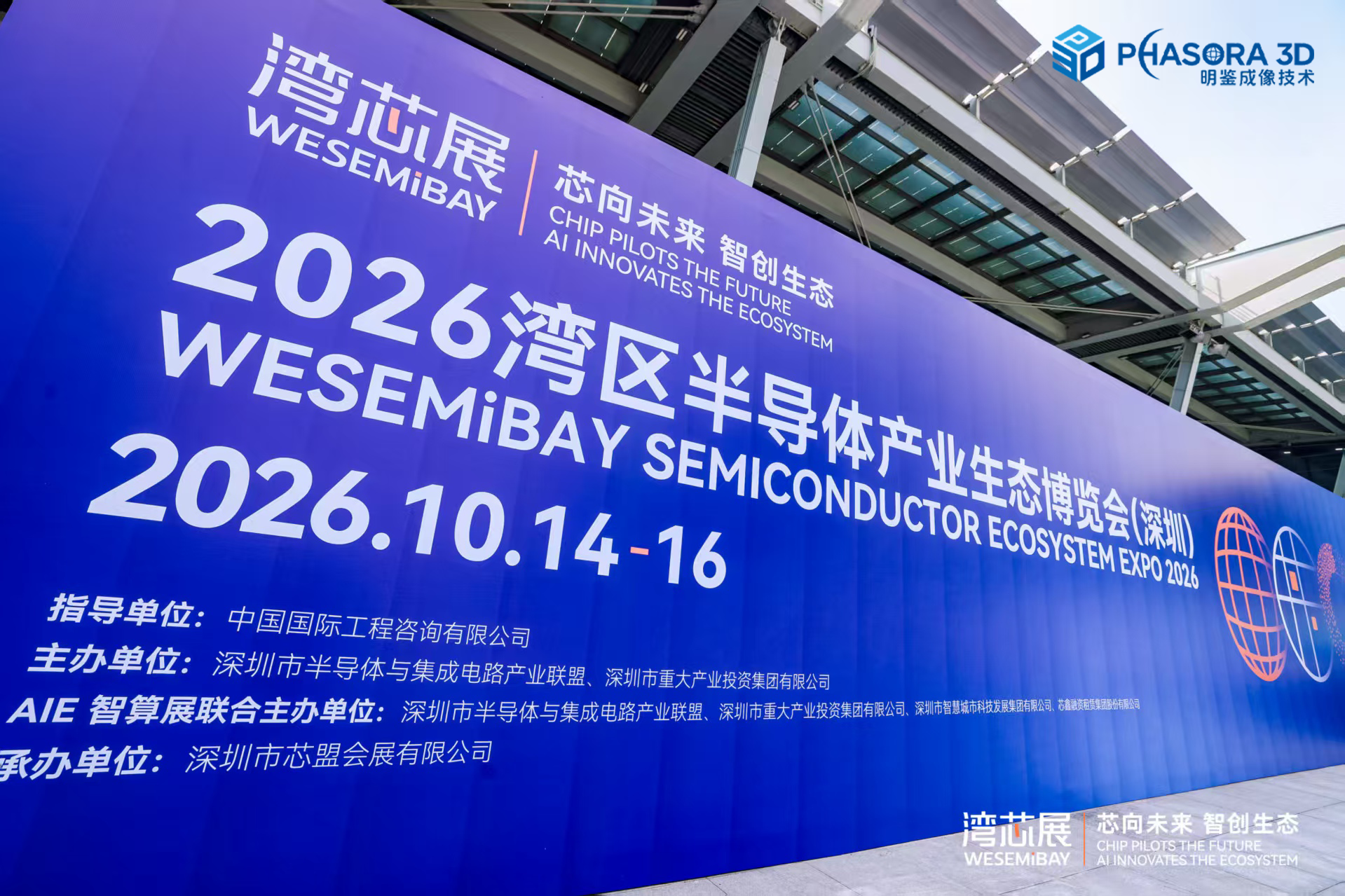
The 2026 Bay Area Semiconductor Industry Ecosystem Expo (Bay Area Chip Expo) concluded on October 16 at the Shenzhen Convention and Exhibition Center (Futian). During the three-day event, Phasora3D Co., Ltd. hosted on-site 3D sample measurements at Booth 7E03, drawing customers who brought their own parts for live data capture.
Visitor samples centered on BGA packages, wire-bond packages, and optical modules — where measurement challenges are most pressing, from solder ball height and coplanarity to fine wire loop height and highly reflective surfaces. With customer expectations shifting from “can it image?” to “can it measure accurately and integrate stably into production?”, we presented three corresponding approaches: a four-camera side-view system for direct solder ball height measurement, optimized imaging for stable fine-wire loop capture at high throughput, and a speed-first solution for optical modules that keeps precision within production-line takt.
Sample measurement requests collected at the expo are now scheduled for follow-up testing with professional reports. Phasora3D Co., Ltd. welcomes customers to visit with samples for on-site measurement verification across advanced packaging, PCBA/SMT, and optical modules.